Asynchronous D flipflop:
--library declaration for the module.
library ieee;
use ieee.std_logic_1164.all;

--This is a D Flip-Flop with Asynchronous Clear and Clock Enable(posedge clock).
--Note that the clear input has the highest priority and
--clock enable having the lowest priority
entity FDCPE1 is
port(Clk :in std_logic;      -- Clock input
    ce :in std_logic;    -- Clock enable input
    clr :in std_logic;  -- Asynchronous clear input
    D :in  std_logic;      -- Data input
    Q : out std_logic      -- Data output
   );
end FDCPE1;

architecture behavioral of FDCPE1 is  --architecture of the circuit.

begin  --"begin" statement for architecture.

process(Clk,clr) --process with sensitivity list.
begin  --"begin" statment for the process.
if(clr = '1') then  --Asynchronous clear input, highest priority
    Q <= '0';
elsif(rising_edge(Clk)) then
    if(ce = '1') then  --clock enable, lowest priority
        Q <= D;
    end if;
end if;
end process;  --end of process statement.

end behavioral;
Testbench Code for the D flipflop:
library ieee;
use ieee.std_logic_1164.all;

--testbench has empty entity
entity tb_FDCPE is
end entity tb_FDCPE;

architecture behavioral of tb_FDCPE is

signal Clk,clr,ce,Q,D : std_logic := '0';
constant Clk_period : time := 10 ns;

begin

--entity instantiation with named association port mapping
FDRSE_uut: entity work.FDCPE1
    port map(Clk => Clk,
        ce => ce,
        clr => clr,
        D => D,
        Q => Q);

--generate clock
Clk_generation: process
begin
    wait for Clk_period/2;
    Clk <= not Clk; --toggle clock when half of clk_period is over
end process;

stimulus: process
begin
    ce <= '1';   D <= '1';  clr <= '0';
    wait for Clk_period;
    D <= '0';   wait for Clk_period;
    D <= '1';   wait for Clk_period;
    clr <= '1';   wait for Clk_period;
    clr <= '0';   wait for Clk_period;
    ce <= '0';  D <= '1'; wait for Clk_period;
    D <= '0'; wait for Clk_period;
    wait;  --testing done. wait endlessly
end process;

end behavioral;
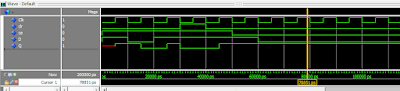
Simulation Waveform from Modelsim:
Schematic from Xilinx Vivado after Synthesis:

Note :- This flipflop entity is named with a "1" at the end because the name "FDCE" stands for a primitive component in Xilinx FPGAs which creates a synthesis error. You can see from the schematic that apart from few input and output buffers, the only flipflop used is called FDCE.
Thank you for your wonderful post but as I am newbie in VHDL.
ReplyDeleteHow about an example of shift register that can increment, shift left , shift right ?
Thanks again ^_^
may not be exactly as per your requirement but I have written code for a PISO shift register here:
ReplyDeletehttp://vhdlguru.blogspot.com/2010/09/examples-for-gate-level-and-behavior.html
Using this you can try to code the module you want.
Can you please post a test bench that could help simulating your code?
ReplyDeleteValue of q is not changing in simulation
ReplyDeleteThis comment has been removed by the author.
Delete