VHDL coding tips and tricks: October 2010

Sunday, October 31, 2010

VHDL: Sequence Detector Using State Machines

    In this article, I want to share the VHDL code for a non-overlapping sequence detector. The code is written using behavioral level modelling and state machines.    

    What is the system that I want to design? I assume that I have an input sequence of bits, arriving at the input port, one bit a time. Whenever the last 4 bits has the value "1011", I want a single pulse to be generated at the output port.

State Machine Diagram:


    The following state machine diagram shows how this works. The VHDL code shared further down in the article is a direct implementation of this state diagram. You can see that the initial state is called "A" and as each incoming bit matches the bit in the sequence "1011", we move to the next state, finally arriving at state "D". The output pulse is generated if the next input bit is '1', matching with the right most bit in the sequence, "1011".

state machine diagram for sequence detector

VHDL Code for Sequence Detector:


library ieee;
use ieee.std_logic_1164.all;

--Sequence detector for detecting the sequence "1011".
--Non overlapping type.
entity sequence_detector is
port(clk : in std_logic;  --clock signal
    reset : in std_logic;   --reset signal
    bit_in : in std_logic;    --serial bit input   
    seq_detected : out std_logic  --A '1' indicates the pattern "1011" is detected in the sequence.
    );
end sequence_detector;

architecture Behavioral of sequence_detector is

type state_type is (A,B,C,D);  --Defines the type for states in the state machine
signal state : state_type := A;  --Declare the signal with the corresponding state type.

begin

process(clk,reset)
begin
    if(reset = '1') then     --resets state and output signal when reset is asserted.
        seq_detected <= '0';
        state <= A;   --initial state
    elsif(rising_edge(clk)) then   --calculates the next state based on current state and input bit.
        case state is
            when A =>   --when the current state is A.
                seq_detected <= '0';
                if(bit_in = '0') then
                    state <= A;
                else   
                    state <= B;  --first bit matches with the 1st bit in "1011" from left.
                end if;
            when B =>   --when the current state is B.
                if(bit_in = '0') then
                    state <= C;  --2nd bit matches with the 2nd bit in "1011" from left.
                else   
                    state <= B;
                end if;
            when C =>   --when the current state is C.
                if(bit_in = '0') then
                    state <= A;
                else   
                    state <= D;  --3rd bit matches with the 3rd bit in "1011" from left.
                end if;
            when D =>   --when the current state is D.
                if(bit_in = '0') then
                    state <= C;
                else   
                    state <= A;
                    --assert pulse on output signal
                    seq_detected <= '1';   --4th bit matches with the final bit in "1011".
                end if;    
            when others =>
                NULL;
        end case;
    end if;
end process;   

end Behavioral;

    I believe that the code is well commented, so I wont explain it any further. Note that, the output depends on the current state and the current input. So what we have just implemented is a Mealy state machine

    The following testbench code was written for testing the code. The sequence "11011101011" was sent to our sequence detector entity, one bit at a time starting from the leftmost bit.

What we are trying to detect is the 4 bit sequence "1011". So an output pulse should be generated on the 5th and the 11th input bit.

My input sequence:  "11011101011".

Testbench Code for Sequence Detector:


library ieee;
use ieee.std_logic_1164.all;

entity tb_sequence_detector is
end tb_sequence_detector;

architecture Behavioral of tb_sequence_detector is

signal clk,reset,bit_in,seq_detected : std_logic := '0';
constant clk_period : time := 10 ns;

begin

    -- entity instantiation with named association
   uut: entity work.sequence_detector port map (
        clk => clk,
        reset => reset,
        bit_in => bit_in,
        seq_detected => seq_detected
        );

   -- generate clock
    clk_process :process
    begin
        wait for clk_period/2;
        clk <= not clk;
    end process;

   -- stimulus process : apply the bits in the sequence one by one.
    stim_proc: process
    begin       
        bit_in <= '1';             --1
        wait for clk_period;
        bit_in <= '1';             --11
        wait for clk_period;
        bit_in <= '0';             --110
        wait for clk_period;
        bit_in <= '1';             --1101
        wait for clk_period;
        bit_in <= '1';             --11011
        wait for clk_period;
        bit_in <= '1';             --110111
        wait for clk_period;
        bit_in <= '0';             --1101110
        wait for clk_period;
        bit_in <= '1';             --11011101
        wait for clk_period;
        bit_in <= '0';             --110111010
        wait for clk_period;
        bit_in <= '1';             --1101110101
        wait for clk_period;
        wait;        
    end process;

end Behavioral;

Simulation Waveform:


The simulated waveform from modelsim is pasted below:

Simulation Waveform for sequence detector in modelsim vhdl


Note:- The code was simulated using modelsim. It was synthesised successfully using AMD Vivado 2023.2 version. 

How to Initialize a Block RAM IP in Xilinx Vivado? (With Testbench)

THIS ARTICLE WAS UPDATED on 19-04-2024. OLD ARTICLE USED XILINX ISE INSTEAD OF VIVADO.

    This article is a continuation of my earlier post, How to use Xilinx Vivado's IP Catalog to create a BRAM? (With Testbench), where I explained the steps to create a Block RAM IP in Xilinx Vivado tool.

    In there, I initialized the bram contents to zero on power up. But you can initialize it with non-zero values as well. How do we do that? It can be done with a special file, which has an extension coe.

    Let me show you how this can be done with few screenshots. Note that you should first follow the instructions from the old article to set up a BRAM as per the settings given there, before proceeding with the rest of this article.

1. In the "Other options" tab in the IP settings, check the checkbox "Load Init File". To add the coe file, click on "Edit" option. Click on "Yes" when the following dialogue box opens up.

create ceo file for bram xilinx vivado

2. Type a filename. I gave the name as "bram_contents.coe". Click on "Save".

3. The following window shows up. Enter the radix of the values. Add the list of values as shown in the screenshot. Click on "Save" and then click on "Close".

how to edit coe file in xilinx vivado

4. Now click on "Ok" and then on "Generate" to generate the IP core.

5. Now we want to test whether the bram is correctly initialized. I have written the following testbench file for this.

library ieee;
use ieee.std_logic_1164.all;

--empty entity for testbench
entity tb_bram is
end tb_bram;

architecture Behavioral of tb_bram is

--copy paste the port declaration of the bram from the xilinx generated file.
component bram_test is
  PORT (
    clka : IN STD_LOGIC;
    ena : IN STD_LOGIC;
    wea : IN STD_LOGIC_VECTOR(0 DOWNTO 0);
    addra : IN STD_LOGIC_VECTOR(7 DOWNTO 0);
    dina : IN STD_LOGIC_VECTOR(7 DOWNTO 0);
    douta : OUT STD_LOGIC_VECTOR(7 DOWNTO 0)
  );
end component;

--port signals for connecting with the bram
signal clka, ena : std_logic := '0';
signal wea : std_logic_vector(0 downto 0) := "0";
signal addra, dina, douta : std_logic_vector(7 downto 0) := (others => '0');
constant clk_period : time := 10 ns; --clock period.

begin

--componenent instantiation using named association.
bram : bram_test port map(
    clka => clka,
    ena => ena,
    wea => wea,
    addra => addra,
    dina => dina,
    douta => douta);

--generate the clock for bram
clk_generation: process
begin
    wait for clk_period/2;
    clka <= not clka;
end process;

--this is where we generate the inputs to apply to the bram
stimulus: process
begin
    wait for clk_period;
    ena <= '1';
    wea <= "0";
    addra <= x"00"; wait for clk_period;
    addra <= x"01"; wait for clk_period;
    addra <= x"02"; wait for clk_period;
    addra <= x"03"; wait for clk_period;
    addra <= x"04"; wait for clk_period;
    addra <= x"05"; wait for clk_period;
    addra <= x"06"; wait for clk_period;
    wait;
end process;

end Behavioral;

6. Once we simulate it, we will get the following simulation waveform. You can see that the first 5 memory locations(addresses 0 to 5) are correctly initialized from 1 to 5, and the rest with zeros.

simulation waveform of bram xilinx vivado


Note :- coe file has different uses. Here we used it to initialize the contents of a BRAM. For an FIR filter, we can use it to specify the filter coefficients.

I have used Xilinx Vivado 2023.2 tool for this article.

If you prefer to see this in action, watch this Youtube video I have created.


Thursday, October 7, 2010

How to use Xilinx Vivado's IP Catalog to create a BRAM? (With Testbench)

THIS ARTICLE WAS UPDATED on 18-04-2024. OLD ARTICLE USED XILINX ISE INSTEAD OF VIVADO.


    BRAM(Block Random access memory) is an advanced memory constructor that generates area and performance-optimized memories using embedded block RAM resources in Xilinx FPGAs. I hope you have already gone through the Core generator introductory tutorial before. If you haven't please read those articles here.


    We will be using Xilinx Vivado 2023.2 version for this. The steps should be the same in any version of Vivado, I believe. Let me guide you through the process with a series of screenshots.

1. Create a new project in Xilinx Vivado.
2. Click on IP Catalog, under flow navigator on the left pane of the software. You will see something like this on screen:


xilinx vivado IP catalog how to start?


2. Type "BRAM" in the search bar and you will get a list of matching results as shown below:


xilinx vivado IP catalog ; search for bram

3. Double click on Block Memory Generator, which is highlighted in the previous screenshot. A new window opens up where you can set the properties of the BRAM. You can check out the data sheet of the BRAM by clicking on Documentation. This is helpful in case you dont understand what these settings are. The component name can be changed as well.


bram IP in xilinx vivado introduction


4. Now we can start customizing the BRAM as per our requirements. Let me share the screenshots of the settings I have chosen.

bram ip in xilinx vivado settings-first page- basic.

bram ip in xilinx vivado settings-second page

bram ip setting from xilinx vivado. initialization file


We have customized our BRAM with the following settings:

  1. It will be of 256 by 8 bits in size.
  2. Algorithm will be chosen for "Low Power".
  3. Read and write width will be of 8 bit.
  4. You can initialize the memory with a coe file, but I have chosen them to be initialized with zeros.


5. Once done, you can click on the summary tab to verify that the settings are correctly chosen.


6. I have set the component name as "bram_test". Now click on the "OK" button at the bottom.

7. Click on "Generate".

generate ip in xilinx vivado

8. The tool will generate the necessary files and will add bram_test as a new source to the project. You should be able to see the new component under "Design Sources".

design sources xilinx vivado

9. Note that double clicking on the .xci file which is highlighted in the above image, will open the IP settings window once again. This means that anytime you can change the bram settings and regenerate the files if you want to.

10. To test the bram entity, we would need its port declaration. Meaning, we would need to know what are the input and output signals, their data type, size etc. To know this, we can click on the arrow, >, which shows the underlying vhdl file. This file contains the port definition which we can copy paste into our testbench code.

vhdl file generated for the ip by vivado xilinx

11. Next step would be to write a testbench code for testing the BRAM we just created. Create a new simulation source (tb_bram.vhd) and copy the following code into it:

library ieee;
use ieee.std_logic_1164.all;

--empty entity for testbench
entity tb_bram is
end tb_bram;

architecture Behavioral of tb_bram is

--copy paste the port declaration of the bram from the xilinx generated file.
component bram_test is
  PORT (
    clka : IN STD_LOGIC;
    ena : IN STD_LOGIC;
    wea : IN STD_LOGIC_VECTOR(0 DOWNTO 0);
    addra : IN STD_LOGIC_VECTOR(7 DOWNTO 0);
    dina : IN STD_LOGIC_VECTOR(7 DOWNTO 0);
    douta : OUT STD_LOGIC_VECTOR(7 DOWNTO 0)
  );
end component;

--port signals for connecting with the bram
signal clka, ena : std_logic := '0';
signal wea : std_logic_vector(0 downto 0) := "0";
signal addra, dina, douta : std_logic_vector(7 downto 0) := (others => '0');
constant clk_period : time := 10 ns; --clock period.

begin

--componenent instantiation using named association.
bram : bram_test port map(
    clka => clka,
    ena => ena,
    wea => wea,
    addra => addra,
    dina => dina,
    douta => douta);

--generate the clock for bram
clk_generation: process
begin
    wait for clk_period/2;
    clka <= not clka;
end process;

--this is where we generate the inputs to apply to the bram
stimulus: process
begin
    wait for clk_period;
    ena <= '1';
    wea <= "1";
    addra <= x"00"; dina <= x"A5";   wait for clk_period;
    addra <= x"04"; dina <= x"B6";   wait for clk_period;
    addra <= x"05"; dina <= x"C7";   wait for clk_period;
    ena <= '0';
    addra <= x"07"; dina <= x"D8";   wait for clk_period;
    wea <= "0";
    ena <= '1';
    addra <= x"00"; wait for clk_period;
    addra <= x"04"; wait for clk_period;
    addra <= x"05"; wait for clk_period;
    addra <= x"07"; wait for clk_period;
    wait;
end process;

end Behavioral;

12. Right click on "tb_bram.vhd" and click on "set as Top". 

13. Run Behavioral Simulation. You should get the following waveform:

simulation waveform of xilinx bram ip in vivado

    You can verify that, when the enable signal ena is low, BRAM doesnt respond to any read or write instruction. Also, there is a 2 clock cycle delay (or latency as they call it) for reading any address from bram. This is as expected as the summary page in the IP generate window says this: "Total port a read Latency: 2 clock cycles".

Note :- What we have tried out here is a very simple BRAM. But it demonstrates how we can work with Xilinx in built IPs. The design will get complicated when you go from single port to dual port RAM's. But the basic idea remains the same. By reading the documentation supplied by Xilinx you can explore more settings used in the GUI tool. For testing purpose I have used Xilinx Vivado 2023.2. The options in the IP tool may vary slightly depending on the version you are using.


If you prefer to see this in action, watch this Youtube video I have created.


Sunday, October 3, 2010

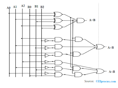
VHDL: 3 bit Magnitude Comparator With Testbench (Gate level Modeling)

    In this post I want to share the VHDL code for a 3 bit comparator which is designed using basic logic gates such as XNOR, OR, AND etc. The code was tested using a self checking testbench which tested the design for all its 64 combinations of inputs.

3 bit Comparator Circuit Diagram:


VHDL code for 3 bit comparator:


library ieee;
use ieee.std_logic_1164.all;

entity comparator is
port(a,b : in std_logic_vector(2 downto 0);  --3 bit numbers to be compared
    a_eq_b : out std_logic;  --a equals b
    a_lt_b : out std_logic;  --a less than b
    a_gt_b : out std_logic   --a greater than b
    );    
end comparator;

architecture gate_level of comparator is

--declare internal signals used in the design
signal temp1,temp2,temp3,temp4,temp5,temp6,temp7,temp8,temp9 : std_logic := '0';

begin

temp1 <= not(a(2) xor b(2));  --XNOR gate with 2 inputs.
temp2 <= not(a(1) xor b(1));  --XNOR gate with 2 inputs.
temp3 <= not(a(0) xor b(0));  --XNOR gate with 2 inputs.
temp4 <= (not a(2)) and b(2);
temp5 <= (not a(1)) and b(1);
temp6 <= (not a(0)) and b(0);
temp7 <= a(2) and (not b(2));
temp8 <= a(1) and (not b(1));
temp9 <= a(0) and (not b(0));

a_eq_b <= temp1 and temp2 and temp3;  -- for a equals b.
a_lt_b <= temp4 or (temp1 and temp5) or (temp1 and temp2 and temp6); --for a less than b
a_gt_b <= temp7 or (temp1 and temp8) or (temp1 and temp2 and temp9); --for a greater than b

end gate_level;

Testbench for 3 bit Comparator:


library ieee;
use ieee.std_logic_1164.all;
--Note that I am using this library only in testbench. Generally its 
--advised to not use this library.
use ieee.std_logic_arith.all;

--testbench has empty entity
entity tb_comparator is
end entity tb_comparator;

architecture behavioral of tb_comparator is

signal a_eq_b,a_lt_b,a_gt_b : std_logic := '0';
signal a,b :std_logic_vector(2 downto 0) := "000";

begin

--entity instantiation with named association port mapping
comparator_uut: entity work.comparator
    port map(a => a,
        b => b,
        a_eq_b => a_eq_b,
        a_lt_b => a_lt_b,
        a_gt_b => a_gt_b);

--self checking testbench. 
--checks for all combinations of inputs.
stimulus: process
begin 
    for i in 0 to 7 loop
        for j in 0 to 7  loop
            --typecast integers to std_logic_vector.
            a <= conv_std_logic_vector(i,3);
            b <= conv_std_logic_vector(j,3);
            wait for 1 ns;
            --the below statements does the automatic verification
            if(a = b) then
                assert a_eq_b = '1';
            elsif(a < b) then
                assert a_lt_b = '1';
            elsif(a > b) then
                assert a_gt_b = '1';
            end if;
        end loop; 
    end loop; 
    wait;  --testing done. wait endlessly
end process;

end behavioral;

Simulation waveform from Modelsim:


3 bit comparator simulation waveform in vhdl modelsim


Post-Synthesis Schematic from Xilinx Vivado:


Post-Synthesis Schematic from Xilinx Vivado for comparator

    You can see that 3 LUT6's were used to implement this logic. As a little homework, why don't you write the behavioral level code for a 3 bit comparator and see if the amount of LUT's used are more or less compared to what we have now. If you do this experiment, let me know the results in the comment section.