VHDL coding tips and tricks: September 2010

Tuesday, September 14, 2010

VHDL: "Generate" Keyword with Examples

    Generate statement is a concurrent statement used in VHDL to describe repetitive structures. You can use generate keyword in your design to instantiate multiple components in just few lines. It can be even combined with conditional statements such as if .. else or iteration statements such as for loops.

    In the first part of this post, I will combine the generate keyword with a for loop to implement a PISO using D flipflops. In fact, in an earlier post, I have done it using individual D flipflop instantiations. You can refer to that code from here, PISO in Gate level and Behavioral level Modeling.

PISO using Generate & for keywords:


--library declaration.
library ieee;
use ieee.std_logic_1164.all;

--parallel in serial out shift register
entity piso is
port(Clk : in std_logic;  --Clock signal
    parallel_in : in std_logic_vector(3 downto 0);  --4 bit parallel load
    load : in std_logic;  --active high for loading the register
    serial_out : out std_logic  --output bit. 
    );
end piso;

architecture gate_level of piso is

signal D,Q : std_logic_vector(3 downto 0) := "0000";

begin

serial_out <= Q(3);

--entity instantiation of the D flipflop using "generate".
F :  --label name
    for i in 0 to 3 generate   --D FF is instantiated 4 times.
    begin  --"begin" statement for "generate"
    ----usual port mapping. Entity instantiation with named association
        FDRSE_inst : entity work.FDRSE1 port map   
            (Clk => Clk,
            ce => '1',
            reset => '0',
            D => D(i),
            set => '0',
            Q => Q(i));  
    end generate F;  --end "generate" block.
--The D inputs of the flip flops are controlled with the load input.
--Two AND gates with a OR gate is used for this.
D(0) <= parallel_in(3) and load;
D(1) <= (parallel_in(2) and load) or (Q(0) and not(load));
D(2) <= (parallel_in(1) and load) or (Q(1) and not(load));
D(3) <= (parallel_in(0) and load) or (Q(2) and not(load));

end gate_level;

The FDRSE flip code can be copied from here: Synchronous D Flip-Flop with Testbench.

I believe that the code is self explanatory. The for loop is used to instantiate as many number of modules as we want to instantiate. To easily port map in a programmatic way, I declare a std_logic_vector for D and Q, and use the index "i" to connect bits of the individual signals to the ports of the individual flipflops.

Johnson Counter using Generate Statement:


    Next I want to show you how to combine generate statement with both if else conditional statement and for loop, to programmatically instantiate multiple components. For this I will be using the example of a Johnson counter.

library ieee;
use ieee.std_logic_1164.all;

entity johnson_counter is
port(clk : in std_logic;
    reset : in std_logic;
    count : out std_logic_vector(3 downto 0)
    );
end johnson_counter;

architecture Behavioral of johnson_counter is

signal D,Q : std_logic_vector(3 downto 0):="0000";
signal not_Q4 : std_logic:='0';

begin

--Q of the last flipflop is fed to the D of the first flop
not_Q4 <= not Q(3);
count <= Q;  --Q is assigned to output port

--generate the instantiation statements for the 4 fliflops
--F,F0 and F1 are label names for the generate statement.
--'generate' statements should have a 'begin' and an 'end'
F : for i in 0 to 3 generate
    begin
        F0 : if (i = 0) generate  --instantiate the "first" FF only.
            begin U1 : entity work.FDRSE1 port map --usual port mapping   
                (Clk => Clk,
                ce => '1',
                reset => reset,
                D => not_Q4,
                set => '0',
                Q => Q(0));     
            end generate F0;
        F1 : if (i > 0) generate --generating the rest of the three FF's.
            begin U2 : entity work.FDRSE1 port map   --usual port mapping
                (Clk => Clk,
                ce => '1',
                reset => reset,
                D => Q(i-1),
                set => '0',
                Q => Q(i));     
            end generate F1;
    end generate F;  
   
end Behavioral;

You can get the testbench for the Johnson counter from this post: 4 bit Johnson Counter with Testbench.
The FDRSE flip code can be copied from here: Synchronous D Flip-Flop with Testbench.

    As you can see from these examples, using "generate" keyword makes your code much more smaller and neat. They even help others to go through and understand your code faster.

    Make sure to visit the older posts linked in the above post to get the testbenches and see screenshots of the simulation waveform.

Monday, September 13, 2010

VHDL: How To Measure The Width Of An Input Pulse

    Is it possible to find the time period of an input pulse? Yes, it is possible and that too with a simple counter, adder and some logic gates. Let's look into how this is done.

    For this to work well, we have to assume that our system clock has a time period much shorter than the width of the pulse we are going to measure. Why so? Because, what we are essentially doing is that, we start a counter when the pulse is High and stop when its Low. The final count, which is when the pulse has just gone Low, gives us the duration of the pulse, in terms of the time period of our clock signal.

    For example, lets say we have a system clock frequency of 100 MHz, which means its time period is 10 ns. If a pulse stays High for 55 ns, the counter would have a final count of 5 by the time the pulse has gone down to Low. 
So we can say that the duration of the pulse = time period of clock * count = 10 ns * 5 = 50 ns.

    Yes, its not correct. But that is unavoidable. This is why I had mentioned that for this to work well, our system clock frequency should be pretty high, compared to that of the input pulse.

    Let us look into the code now:

Pulse Duration Counter:


library ieee;
use ieee.std_logic_1164.all;
use ieee.numeric_std.all;

entity pulse_duration_counter is
port(clk : in std_logic;
    pulse_in : in std_logic;
    valid_output : out std_logic;
    pulse_duration : out unsigned(47 downto 0)
    );
end pulse_duration_counter;

architecture Behavioral of pulse_duration_counter is

--In VHDL-1997, output ports cannot be read. Thats why we use temp here.
signal temp : unsigned(47 downto 0) := (others => '0');

begin

process(clk)
begin
if(rising_edge(clk)) then
    if (pulse_in = '1') then 
        temp <= temp + 1;
        valid_output <= '0';
        --signals get their values updated only at the end of the process.
        --thats why I have to add '1' to temp before assigning it as output.
    else
        pulse_duration <= temp; 
        if(temp > 0) then
            valid_output <= '1';
        else
            valid_output <= '0';
        end if;
        temp <= (others => '0');
    end if;
end if;
end process;
   
end Behavioral;

Testbench for Pulse Duration Counter:


library ieee;
use ieee.std_logic_1164.all;
use ieee.numeric_std.all;

--testbench has empty entity
entity tb_pulse_counter is
end entity tb_pulse_counter;

architecture behavioral of tb_pulse_counter is

signal clk,pulse_in,valid_output : std_logic := '0';
signal pulse_duration :unsigned(47 downto 0) := (others => '0');
constant clk_period : time := 10 ns;

begin

--entity instantiation with named association port mapping
pulse_counter_uut: entity work.pulse_duration_counter
    port map(clk => clk,
        pulse_in => pulse_in,
        valid_output => valid_output,
        pulse_duration => pulse_duration);

--generate clock
Clk_generation: process
begin
    wait for clk_period/2;
    clk <= not clk; --toggle clock when half of clk_period is over
end process;

stimulus: process
begin 
    pulse_in <= '0';    wait for Clk_period;
    pulse_in <= '1';    wait for Clk_period*10;
    pulse_in <= '0';    wait for Clk_period*2;
    pulse_in <= '1';    wait for Clk_period*20;
    pulse_in <= '0';    wait for Clk_period*5;
    pulse_in <= '1';    wait for Clk_period*15;
    pulse_in <= '0';    
    wait;  --testing done. wait endlessly
end process;

end behavioral;

Simulation waveform from Modelsim:


simulation waveform of pulse counter from modelsim vhdl


Synthesis:


The pulse duration counter entity was synthesised successfully using Xilinx Vivado 2023.2. 

Notes:


    We can create many variations for this design. The current counter only counts the duration of the High pulse. We could make it so that both High and Low pulse widths are counted. 

    If our pulses arent going to be High for very long, we could decrease the size of the counter from 48 bits to something smaller, say 16 bits. I had used a width of 48 bits, keeping in mind of an extreme usage case. 

VHDL: 4 bit Johnson Counter with Testbench

    A Johnson counter is a digital circuit which consists of a series of flip flops connected together in a feedback manner. This is very similar to a ring counter with just one tiny difference. The circuit is special type of shift register where the complement output of the last flipflop is fed back to the input of first flipflop. When the circuit is reset, all the flipflop outputs are made zero. With a n-flipflop Johnson counter we get a MOD-2n counter. That means the counter has 2n different states.

Block Diagram:


The circuit diagram for a 3 bit Johnson counter is shown below:

block diagram for 3 bit johnson counter

     
    The counter goes through the following states over and over when the reset is not applied: 001  -   011  -  111   -   110  -  100  - 000  ...

Johnson Counter:


library ieee;
use ieee.std_logic_1164.all;

entity johnson_counter is
port(clk : in std_logic;
    reset : in std_logic;
    count : out std_logic_vector(3 downto 0)
    );
end johnson_counter;

architecture Behavioral of johnson_counter is

signal temp : std_logic_vector(3 downto 0) := (others => '0');

begin

--assign the temparary signal to output port.
--In VHDL-1997, output ports cannot be read. Thats why we use temp here.
count <= temp; 

process(clk)
begin
if(rising_edge(clk)) then
    if (reset = '1') then ---synchronous reset
        temp <= (others => '0');
    else
        --these are concurrent statements. 
        --which means they all execute at the same time.
        temp(1) <= temp(0);
        temp(2) <= temp(1);
        temp(3) <= temp(2);
        temp(0) <= not temp(3);
    end if;
end if;
end process;
   
end Behavioral;

Testbench for the Johnson Counter:


library ieee;
use ieee.std_logic_1164.all;

--testbench has empty entity
entity tb_johnson_counter is
end entity tb_johnson_counter;

architecture behavioral of tb_johnson_counter is

signal clk,reset : std_logic := '0';
signal count :std_logic_vector(3 downto 0) := "0000";
constant clk_period : time := 10 ns;

begin

--entity instantiation with named association port mapping
counter_uut: entity work.johnson_counter
    port map(clk => clk,
        reset => reset,
        count => count);

--generate clock
Clk_generation: process
begin
    wait for clk_period/2;
    clk <= not clk; --toggle clock when half of clk_period is over
end process;

stimulus: process
begin 
    reset <= '1';  wait for clk_period;
    reset <= '0';   wait for Clk_period*10;
    reset <= '1';   wait for Clk_period;
    reset <= '0';   
    wait;  --testing done. wait endlessly
end process;

end behavioral;

Lets take a look at the simulation waveform from modelsim.

Simulation Waveform from Modelsim:


johnson counter simulation waveform from modelsim vhdl

Post Synthesis Schematic from Xilinx Vivado:


The schematic looks quite simple, few flipflops connected in a sequence, along with some input and output buffers.

technology schematic for 4 bit johnson counter

VHDL: 4 bit Ring Counter with Testbench

    A ring counter is a digital circuit which consists of a series of flip flops connected together in a feedback manner. This circuit is a special type of shift register where the output of the last flipflop is fed back to the input of the first flipflop. When the circuit is reset, except one of the flipflop output, all others are made zero. For n-flipflop ring counter we have a MOD-n counter. That means the counter has n different states.

Block Diagram:


The circuit diagram for a 4 bit ring counter is shown below:

block diagram for ring counter

     
    The counter goes through the following states over and over when the reset is not applied: 0001  -   0010   -  0100   -   1000 ...

Ring Counter:


library ieee;
use ieee.std_logic_1164.all;

entity ring_counter is
port(clk : in std_logic;
    reset : in std_logic;
    count : out std_logic_vector(3 downto 0)
    );
end ring_counter;

architecture Behavioral of ring_counter is

signal temp : std_logic_vector(3 downto 0) := (others => '0');

begin

--assign the temparary signal to output port.
--In VHDL-1997, output ports cannot be read. Thats why we use temp here.
count <= temp; 

process(clk)
begin
if(rising_edge(clk)) then
    if (reset = '1') then ---synchronous reset
        temp <= (0=> '1', others => '0');
    else
        --these are concurrent statements. 
        --which means they all execute at the same time.
        temp(1) <= temp(0);
        temp(2) <= temp(1);
        temp(3) <= temp(2);
        temp(0) <= temp(3);
    end if;
end if;
end process;
   
end Behavioral;

Testbench for the Ring Counter:


library ieee;
use ieee.std_logic_1164.all;

--testbench has empty entity
entity tb_ring_counter is
end entity tb_ring_counter;

architecture behavioral of tb_ring_counter is

signal clk,reset : std_logic := '0';
signal count :std_logic_vector(3 downto 0) := "0000";
constant clk_period : time := 10 ns;

begin

--entity instantiation with named association port mapping
counter_uut: entity work.ring_counter
    port map(clk => clk,
        reset => reset,
        count => count);

--generate clock
Clk_generation: process
begin
    wait for clk_period/2;
    clk <= not clk; --toggle clock when half of clk_period is over
end process;

stimulus: process
begin 
    reset <= '1';  wait for clk_period;
    reset <= '0';   wait for Clk_period*6;
    reset <= '1';   wait for Clk_period;
    reset <= '0';   
    wait;  --testing done. wait endlessly
end process;

end behavioral;

Lets take a look at the simulation waveform from modelsim.

Simulation Waveform from Modelsim:


ring counter simulation waveform from modelsim vhdl

Post Synthesis Schematic from Xilinx Vivado:


The schematic looks quite simple, few flipflops connected in a sequence, along with some input and output buffers.
technology schematic for 4 bit ring counter


Thursday, September 9, 2010

VHDL: Parallel In Serial Out Register with Testbench

    In this article I want to share the VHDL code for a 4 bit parallel in serial out shift register. Its known as PISO in short form. The shift register can be loaded with any chosen 4 bit value and thereafter in every clock cycle a bit is shifted out from the output port.

    To make it interesting, I have written two different versions of the code - one in behavioral level and in another in gate level. This will help you understand practically, how these two models are different. 

    In gate level modeling the entity is implemented in terms of logic gates and their interconnections. Designs at this level are similar to describing a circuit in terms of a gate level logic diagram.

    In Behavioral level(Algorithmic level) modeling an entity is implemented in terms of the desired design algorithm without the concern for the hardware circuit elements. Designing at this level is the highest abstraction level provided by VHDL.

    Lets look at the Behavioral level model for PISO first. Its much easier to understand than the gate level, I believe.

PISO - Behavioral Level Model:


--library declaration.
library ieee;
use ieee.std_logic_1164.all;

--parallel in serial out shift register
entity piso is
port(Clk : in std_logic;  --Clock signal
    parallel_in : in std_logic_vector(3 downto 0);  --4 bit parallel load
    load : in std_logic;  --active high for loading the register
    serial_out : out std_logic  --output bit. 
    );
end piso;

architecture behavioral of piso is

signal load_value : std_logic_vector(3 downto 0) := "0000";

begin

process(Clk)
begin
if(rising_edge(Clk)) then
    if(load ='0') then  --do the serial right shifting here.
        serial_out <= load_value(3); --MSB goes to output port
        load_value(3) <= load_value(2);
        load_value(2) <= load_value(1);
        load_value(1) <= load_value(0);
        load_value(0) <= '0';  --'0' is loaded to LSB
    else   --load the registers with a new value to shift.
        load_value <= parallel_in;
    end if;
end if;
end process;

end behavioral;

Testbench for the PISO:


library ieee;
use ieee.std_logic_1164.all;

--testbench has empty entity
entity tb_piso is
end entity tb_piso;

architecture behavioral of tb_piso is

signal Clk,load,serial_out : std_logic := '0';
signal parallel_in :std_logic_vector(3 downto 0) := "0000";
constant Clk_period : time := 10 ns;

begin

--entity instantiation with named association port mapping
piso_uut: entity work.piso
    port map(Clk => Clk,
        parallel_in => parallel_in,
        load => load,
        serial_out => serial_out);

--generate clock
Clk_generation: process
begin
    wait for Clk_period/2;
    Clk <= not Clk; --toggle clock when half of clk_period is over
end process;

stimulus: process
begin 
    wait for Clk_period;
    parallel_in <= "1011";  wait for Clk_period;
    load <= '1';   wait for Clk_period;
    load <= '0';   wait for Clk_period*5;
    parallel_in <= "1001";  wait for Clk_period;
    load <= '1';   wait for Clk_period;
    load <= '0';   wait for Clk_period*5;
    wait;  --testing done. wait endlessly
end process;

end behavioral;

Lets take a look at the simulation waveform from modelsim.

Simulation Waveform from Modelsim:


piso simulation waveform from modelsim vhdl

Post Synthesis Schematic from Xilinx Vivado:


technology schematic from xilinx vivado for piso

PISO - Gate Level Model:


    Looking at the first code, you can see that the it is written using if.. else.. statements. We haven't used any digital circuit elements like flip-flops, gates or registers. The code describes what we want, in a language similar to a high level language like C (though there are lot of differences between C and VHDL).

Now let us look at the Gate level code:

--library declaration.
library ieee;
use ieee.std_logic_1164.all;

--parallel in serial out shift register
entity piso is
port(Clk : in std_logic;  --Clock signal
    parallel_in : in std_logic_vector(3 downto 0);  --4 bit parallel load
    load : in std_logic;  --active high for loading the register
    serial_out : out std_logic  --output bit. 
    );
end piso;

architecture gate_level of PISO is

signal D1,D2,D3,D4,Q1,Q2,Q3,Q4 : std_logic := '0';
signal load_value : std_logic_vector(3 downto 0) := "0000";

begin

load_value <= parallel_in;
serial_out <= Q4;

--entity instantiation of the D flipflop.It is instantiated 4 times to make a 4 bit register.
FDRSE11 : entity work.FDRSE1    
    port map (
        Clk => Clk,
        ce => '1',
        reset => '0',
        D => D1,
        set => '0',
        Q => Q1);  --MSB

FDRSE22 : entity work.FDRSE1
port map (
    Clk => Clk,
    ce => '1',
    reset => '0',
    D => D2,
    set => '0',
    Q => Q2);

FDRSE33 : entity work.FDRSE1
    port map (
        Clk => Clk,
        ce => '1',
        reset => '0',
        D => D3,
        set => '0',
        Q => Q3);

FDRSE44 : entity work.FDRSE1  
    port map (
        Clk => Clk,
        ce => '1',
        reset => '0',
        D => D4,
        set => '0',
        Q => Q4);   --LSB

--The D inputs of the flip flops are controlled with the load input.
--Two AND gates with a OR gate is used for this.
D1 <= load_value(3) and load;
D2 <= (load_value(2) and load) or (Q1 and not(load));
D3 <= (load_value(1) and load) or (Q2 and not(load));
D4 <= (load_value(0) and load) or (Q3 and not(load));

end gate_level;

The FDRSE1 flipflop used in the above code can be copied from an earlier post: Synchronous D Flip-Flop with Testbench.

    We can make the following observations from the code:
  1. The D flipflop itself is written in behavioral level, but that doesnt matter, since its instantiated as a "black box" in the piso entity.
  2. We have used VHDL gate level primitives such as not, and, or etc.. to implement our design.
  3. The flip flop required for implementing the 4 bit register was defined in a separate file and then instantiated in the piso entity. 
  4. We didn't use a "process" statement in the code.
  5. The above code is also an example of Structural level modeling, where we use a hierarchy of entities. For example the D flip flop is considered as a black box from the PISO block's point of view. Once the flip flop (or generally any other module) is designed and verified we can use it any number of times anywhere as part of another design. 

    Another example for structural level coding : 4 bit Synchronous UP counter(with reset) using JK flip-flops. 
    
    Some more examples for gate level modeling: 3 to 8 decoder using basic logic gates and 4 bit ripple carry adder.

Lets take a look at the simulation waveform from modelsim.

Simulation Waveform from Modelsim:


simulation waveform in modelsim of piso vhdl


Post Synthesis Schematic from Xilinx Vivado:


schematic of piso from xilinx vivado vhdl


I hope, by this point, the differences between Behavioral and Gate level modeling is clear to you. Those who have come to the field of FPGAs from a software engineering background, might find it hard to do gate level designs. But it doesn't really matter. Often you can write equally efficient designs using behavioral modelling, if you keep few fundamental facts of hardware designing in mind.

Note:- I have instantiated modules using the "entity instantiation" method. If you are new to this method please read this article, Instantiating components in VHDL.

Wednesday, September 8, 2010

VHDL: Asynchronous D Flip-Flop with Testbench

    As per the request from few readers I have decided to post some simple VHDL codes for people who are just starting out with VHDL. This, here is a D Flip-Flop with Asynchronous Clear and Clock Enable(posedge clock). The code is well commented I believe, so I wont bore you with more explanations.

Asynchronous D flipflop:


--library declaration for the module.
library ieee;
use ieee.std_logic_1164.all;

--This is a D Flip-Flop with Asynchronous Clear and Clock Enable(posedge clock).
--Note that the clear input has the highest priority and 
--clock enable having the lowest priority
entity FDCPE1 is
port(Clk :in std_logic;      -- Clock input
    ce :in std_logic;    -- Clock enable input
    clr :in std_logic;  -- Asynchronous clear input
    D :in  std_logic;      -- Data input
    Q : out std_logic      -- Data output
   );
end FDCPE1;

architecture behavioral of FDCPE1 is  --architecture of the circuit.

begin  --"begin" statement for architecture.

process(Clk,clr) --process with sensitivity list.
begin  --"begin" statment for the process.
if(clr = '1') then  --Asynchronous clear input, highest priority
    Q <= '0';
elsif(rising_edge(Clk)) then  
    if(ce = '1') then  --clock enable, lowest priority
        Q <= D;      
    end if;
end if;     
end process;  --end of process statement.

end behavioral;

Testbench Code for the D flipflop:

library ieee;
use ieee.std_logic_1164.all;

--testbench has empty entity
entity tb_FDCPE is
end entity tb_FDCPE;

architecture behavioral of tb_FDCPE is

signal Clk,clr,ce,Q,D : std_logic := '0';
constant Clk_period : time := 10 ns;

begin

--entity instantiation with named association port mapping
FDRSE_uut: entity work.FDCPE1
    port map(Clk => Clk,
        ce => ce,
        clr => clr,
        D => D,
        Q => Q);

--generate clock
Clk_generation: process
begin
    wait for Clk_period/2;
    Clk <= not Clk; --toggle clock when half of clk_period is over
end process;

stimulus: process
begin
    ce <= '1';   D <= '1';  clr <= '0';   
    wait for Clk_period;
    D <= '0';   wait for Clk_period;
    D <= '1';   wait for Clk_period;
    clr <= '1';   wait for Clk_period;
    clr <= '0';   wait for Clk_period;
    ce <= '0';  D <= '1'; wait for Clk_period;  
    D <= '0'; wait for Clk_period;  
    wait;  --testing done. wait endlessly
end process;

end behavioral;

Simulation Waveform from Modelsim:


simulation waveform of d flipflop in vhdl, modelsim

Schematic from Xilinx Vivado after Synthesis:


technology schematic from xilinx vivado of d flipflop


Note :- This flipflop entity is named with a "1" at the end because the name "FDCE" stands for a primitive component in Xilinx FPGAs which creates a synthesis error. You can see from the schematic that apart from few input and output buffers, the only flipflop used is called FDCE.

VHDL: Synchronous D Flip-Flop with Testbench

   As per the request from few readers I have decided to post some simple VHDL codes for people who are just starting out with VHDL. This, here is a D Flip-Flop with Synchronous Reset, Set and Clock Enable(posedge clock). The code is well commented I believe, so I wont bore you with more explanations.

Synchronous D flipflop:


--library declaration for the module.
library ieee;
use ieee.std_logic_1164.all;

--This is a D Flip-Flop with Synchronous Reset,Set and Clock Enable(posedge clk).
--Note that the reset input has the highest priority,Set being the next highest
--priority and clock enable having the lowest priority.
entity FDRSE1 is
port(Clk :in std_logic;      -- Clock input
    ce :in std_logic;    -- Clock enable input
    reset :in std_logic;  -- Synchronous reset input
    D :in  std_logic;      -- Data input
    set : in std_logic;   -- Synchronous set input
    Q : out std_logic      -- Data output
   );
end FDRSE1;

architecture behavioral of FDRSE1 is  --architecture of the circuit.

begin  --"begin" statement for architecture.

process(Clk) --process with sensitivity list.
begin  --"begin" statment for the process.
    if(rising_edge(Clk)) then  --This makes the process synchronous(with clock)
        if(reset = '1') then  --synchronous reset, highest priority
            Q <= '0';
        else
            if(set = '1') then  --synchronous set, next priority
                Q <= '1';
            else
                if(ce = '1') then   --clock enable, lowest priority
                    Q <= D;      
                end if;
            end if;
        end if;
    end if;      
end process;  --end of process statement.

end behavioral;

Testbench Code for the D flipflop:

library ieee;
use ieee.std_logic_1164.all;

--testbench has empty entity
entity tb_FDRSE is
end entity tb_FDRSE;

architecture behavioral of tb_FDRSE is

signal Clk,reset,ce,Q,D,set : std_logic := '0';
constant Clk_period : time := 10 ns;

begin

--entity instantiation with named association port mapping
FDRSE_uut: entity work.FDRSE1 
    port map(Clk => Clk,
        ce => ce,
        reset => reset,
        D => D,
        set => set,
        Q => Q);

--generate clock
Clk_generation: process
begin
    wait for Clk_period/2;
    Clk <= not Clk; --toggle clock when half of clk_period is over
end process;

stimulus: process
begin
    ce <= '1';   D <= '1';  
    set <= '0';     reset <= '0';   
    wait for Clk_period;
    D <= '0';   wait for Clk_period;
    D <= '1';   wait for Clk_period;
    reset <= '1';   wait for Clk_period;
    reset <= '0';   wait for Clk_period;
    set <= '1';   wait for Clk_period;
    set <= '0';   D <= '0'; wait for Clk_period;
    ce <= '0';  D <= '1'; wait for Clk_period;  
    wait;  --testing done. wait endlessly
end process;

end behavioral;

Simulation Waveform from Modelsim:


simulation waveform of d flipflop in vhdl, modelsim

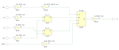
Schematic from Xilinx Vivado after Synthesis:


technology schematic from xilinx vivado of d flipflop


Note :- This flipflop entity is named with a "1" at the end because the name "FDRSE" stands for a primitive component in Xilinx FPGAs which creates a synthesis error. You can see from the schematic that apart from few logic gates, the only flipflop used is called FDRE.