VHDL coding tips and tricks: Gate level model
Showing posts with label Gate level model. Show all posts

Friday, November 6, 2020

Quaternary Signed Digit (QSD) Based Fast Adder In VHDL

    Quaternary Signed Digit is a base-4 number system where a number is represented by one of the following 7 digits : -3,-2,-1,0,1,2,3. The advantage of this number system is that it allows carry free addition, thus speeding up the addition process.

    Fast adders based on QSD are typical and there are several papers on this. In this post I have written the VHDL code for a 4 digit(each input being 12 bits) QSD adder. With a bit of editing, this code can be extended to handle larger input numbers.

    One thing to be careful about is that while checking online for information on QSD adders, I came upon several papers with some little mistakes here and there. Even though these typos are small, but it can take hours of your debugging time, as it did in my case. So I recommend cross checking any circuit diagram you see online across several references.

The Block diagram for the design is given below:


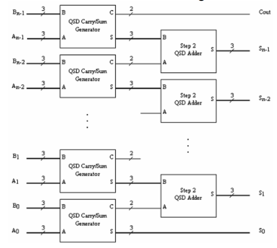
A QSD adder has two stages. 

In the first stage we perform operation on a single digit from each operand to form an intermediate carry and sum. The carry is 2 bit and can have one of the three values from -1 to +1. 
The sum is 3 bit and can have one of the 7 values from -3 to +3.

In the second stage, the intermediate carry and sum are simply added to form a single 3 bit sum which is between -3 to +3.

For an N digit QSD adder we have two input operands each N*3 bit in size. The Carry output is 2 bit in size and Sum output is N*3 bit in size. 

For a N digit QSD adder we need N carry-sum generators and N-1 adders. How these blocks are connected together are shown in the block diagram above.

The boolean equations for these blocks are available in Page 4 of the second pdf shared in this blog. But some of these equations are not correct. But the circuit diagram given in the page 5 of the same pdf is correct and you can refer it to form the correct boolean equations.

The carry sum generator can be better understood by looking at the Table 2 and 3 of the first pdf. And table 5 gives more clarity on how the second step adder is working.

The VHDL codes are given below:

First step : Carry Sum Generator

--QSD carry sum generator.
library IEEE;
use IEEE.STD_LOGIC_1164.ALL;
use IEEE.NUMERIC_STD.ALL;

entity QSD_cs_gen is
    Port ( A,B : in  signed(2 downto 0);
           S : out  signed(2 downto 0);
	   		C : out  signed(1 downto 0)	
	);
end QSD_cs_gen;

architecture Behavioral of QSD_cs_gen is

begin

process(A,B)
variable anot,bnot : signed(2 downto 0);
variable ss : signed(2 downto 0);
variable cc : signed(1 downto 0);
variable temp1,temp2,temp3,temp4,temp5 : std_logic;
begin
	anot := not A;
	bnot := not B;
	temp1 := not(A(1) or B(1));
	temp2 := A(2) and bnot(0);
	temp3 := B(2) and anot(0);
	temp4 := temp1 and (temp2 or temp3);
	cc(1) := (A(2) and B(2) and not(A(0) and B(0) and A(1) and B(1))) or temp4;
	cc(0) := cc(1) or ((anot(2) and bnot(2)) and 
			((A(1) and B(1)) or (B(1) and B(0)) or (B(1) and A(0)) or (B(0) and A(1)) or (A(1) and A(0))));

	ss(0) := A(0) xor B(0);
	ss(1) := A(1) xor B(1) xor (A(0) and B(0));
	temp1 := (ss(0) and (A(1) xor B(1)));
	temp2 := (B(2) and anot(1) and bnot(0));
	temp3 := (A(2) and bnot(1) and anot(0));
	temp4 := ( A(0) and B(0) and anot(1) and bnot(1) and (A(2) or B(2)) );
	temp5 := ( A(0) and B(0) and A(1) and B(1) and A(2) and B(2) );
	ss(2) := temp1 or temp2 or temp3 or temp4 or temp5;

	S <= ss;
	C <= cc;
end process;

end Behavioral;


Second step : Addition of Intermediate Carry and Sum


--QSD step 2: adder for adding intermediate carry and sum.
library IEEE;
use IEEE.STD_LOGIC_1164.ALL;
use IEEE.NUMERIC_STD.ALL;

entity QSD_adder is
    Port ( A : in  signed(1 downto 0);
           B : in  signed(2 downto 0);
	   	   S : out  signed(2 downto 0)	
	);
end QSD_adder;

architecture Behavioral of QSD_adder is

begin

process(A,B)
variable sum : signed(2 downto 0);
variable temp1,temp2,temp3,temp4 : std_logic;
begin
	sum(0) := A(0) xor B(0);
	sum(1) := A(1) xor B(1) xor (A(0) and B(0));
	temp1 := A(1) and B(1);
	temp2 := A(1) xor B(1);
	temp3 := A(0) and B(0);
	temp4 := temp1 or (temp2 and temp3);
	sum(2) := A(1) xor B(2) xor temp4;
	S <= sum;
end process;

end Behavioral;


4 Digit QSD Adder:

--4 digit QSD adder. 
library IEEE;
use IEEE.STD_LOGIC_1164.ALL;
use IEEE.NUMERIC_STD.ALL;

entity QSDAdder is
    Port ( A,B : in  signed(11 downto 0);
           Cout : out  signed(1 downto 0);
	   	   S : out  signed(11 downto 0)	
	);
end QSDAdder;

architecture Behavioral of QSDAdder is
 
component QSD_cs_gen is
    Port ( A,B : in  signed(2 downto 0);
           S : out  signed(2 downto 0);
	   		C : out  signed(1 downto 0)	
	);
end component;

component QSD_adder is
    Port ( A : in  signed(1 downto 0);
           B : in  signed(2 downto 0);
	   	   S : out  signed(2 downto 0)	
	);
end component;

signal S0,S1,S2,S3 : signed(2 downto 0);
signal C0,C1,C2,C3 : signed(1 downto 0);

begin

--First stage to QSD addition : The 4 carry-sum generators.
carry_sum_gen1 : QSD_cs_gen port map (
          A => A(2 downto 0),
          B => B(2 downto 0),
		  S => S(2 downto 0),
		  C => C0
        );

carry_sum_gen2 : QSD_cs_gen port map (
          A => A(5 downto 3),
          B => B(5 downto 3),
		  S => S1,
		  C => C1
        );

carry_sum_gen3 : QSD_cs_gen port map (
          A => A(8 downto 6),
          B => B(8 downto 6),
		  S => S2,
		  C => C2
        );

carry_sum_gen4 : QSD_cs_gen port map (
          A => A(11 downto 9),
          B => B(11 downto 9),
		  S => S3,
		  C => Cout
        );
 
--Second stage to QSD addition : The addition of intermediate carry's and sum's
adder1 : QSD_adder port map (
          A => C0,
          B => S1,
		  S => S(5 downto 3)
        );

adder2 : QSD_adder port map (
          A => C1,
          B => S2,
		  S => S(8 downto 6)
        );

adder3 : QSD_adder port map (
          A => C2,
          B => S3,
		  S => S(11 downto 9)
        );


end Behavioral;


Testbench for the 4 Digit QSD Adder:

--Testbench code which tests all combinations of inputs to a 4 digit QSD adder
library IEEE;
use IEEE.Std_logic_1164.all;
use IEEE.Numeric_Std.all;

entity QSDAdder_tb is
end;

architecture bench of QSDAdder_tb is

  component QSDAdder
      Port ( A,B : in  signed(11 downto 0);
             Cout : out  signed(1 downto 0);
  	   	    S : out  signed(11 downto 0)	
  	);
  end component;

  signal A,B: signed(11 downto 0);
  signal Cout: signed(1 downto 0);
  signal S: signed(11 downto 0) ;

	--A function to convert any length QSD number to a signed integer.
	function  qsd2int  ( A : SIGNED ) return signed is

	variable res : signed(31 downto 0) := (others => '0');
	variable num_digits : integer := (A'high+1)/3;
	variable temp : signed(31 downto 0) := (others => '0');
	variable ones : signed(31 downto 0) := (others => '1');
	variable zeros : signed(31 downto 0) := (others => '0');
	
	begin
	for i in 0 to num_digits-1 loop
		if(A(2+3*i) = '1') then  --this part is just does sign extension
			temp := ones(31 downto 3) & A(2+3*i downto 3*i);
		else
			temp := zeros(31 downto 3) & A(2+3*i downto 3*i);
		end if;
		res := res + shift_left(temp,2*i); --shift left and accumulate.
	end loop;
	return res;
	
	end qsd2int;
  
signal A_dec,B_dec,S_dec,S_act : signed(31 downto 0) := (others => '0');
signal error : integer := 0;

begin

  uut: QSDAdder port map ( A    => A,
                           B    => B,
                           Cout => Cout,
                           S    => S );

 --this is where we generate inputs to apply to the adder.
 --4 digits for one number. and we have two numbers. 
 --so 8 for-loops to generate all combination of values for all digits.
  stimulus: process
  begin
	wait for 5 ns;
	for i in -3 to 3 loop
  		for j in -3 to 3 loop
			for k in -3 to 3 loop
				for l in -3 to 3 loop
					A <= to_signed(i,3) & to_signed(j,3) & to_signed(k,3) & to_signed(l,3);
					for m in -3 to 3 loop
				  		for n in -3 to 3 loop
							for o in -3 to 3 loop
								for p in -3 to 3 loop
									B <= to_signed(m,3) & to_signed(n,3) & to_signed(o,3) & to_signed(p,3);	
									wait for 10 ns;
								end loop;									
							end loop;
						end loop;
					end loop;
				end loop;
			end loop;
		end loop;
	end loop;
	wait;
  end process;

--the outputs are checked here for error with actual sum.
check_results: process
variable A_dec1,B_dec1,S_dec1,S_act1 : signed(31 downto 0) := (others => '0');
begin
	for i in 1 to 7**8 loop  --7^8 total set of inputs.
		wait for 10 ns;
		A_dec1 := qsd2int(A);
		B_dec1 := qsd2int(B);
		--if carry out is -1 we subtract 256. or else we add if carry out is 1.
		if(Cout = "11") then  
			S_dec1 := qsd2int(S)-256;
		elsif(Cout = "01") then
			S_dec1 := qsd2int(S)+256;
		else  --carry out is zero.
			S_dec1 := qsd2int(S);
		end if;
		S_act1 := A_dec1+B_dec1;
		--if result from adder and actual sum doesnt match increment "error"
		if(S_dec1 /= S_act1) then
			error <= error+1;  
		end if;
		A_dec <= A_dec1;
		B_dec <= B_dec1;
		S_dec <= S_dec1;
		S_act <= S_act1;
	end loop;
	wait;
end process;

end;

    A bit of explanation on the VHDL codes:

    The first two codes, QSD_cs_gen and QSD_adder, are simply based on the boolean equations and circuit diagram presented in the second pdf. Its a gate level code. Note that I have broken the long equations into several lines by using temporary variables. This adds clarity as well as makes the code you write less prone to error.

    The third code, QSDAdder, is the 4 digit QSD adder, which connects the above two blocks in a structural level design.

    The fourth code, QSDAdder_tb, is the testbench for testing the functionality of our adder. This is relatively complicated compared to the other three blocks of code.

    Testbench has a function named qsd2int, which converts any QSD number into a signed number. Each digit of the QSD number is sign extended to 32 bits and then left shifted by a multiple of 2 before accumulatively adding to the result. Left shifting here simply means I am trying to multiply by 1,4,16,64 etc. based on the index of the digit.
    In the testbench I want to test the design for all the possible combinations of inputs. There are two 4 digit QSD numbers and each number has 7 possible values.  Which means that the number of sets of inputs is 7^(4+4) = 7^8 = 5764801. This is achieved in the process named stimulus.
    The resultant sum from the Adder module are compared with the actual result in another process named check_results. If there is a mismatch in this comparison, a variable named error is incremented by 1. The Adder is fully working, if by the end of the simulation error is still 0.

    VHDL codes and papers which I have referred to write the codes can be downloaded as a Zipped file from here

    Note that the Boolean equations in the second paper have some mistakes. But you can check the circuit diagram, which seems to be correct. Cross check with the VHDL codes if you are not sure. 

    The codes were simulated and tested successfully using Modelsim 10.4a.

Sunday, October 29, 2017

Count the number of 1's in a Binary number - Circuit design and VHDL implementation

Suppose you have a binary number, how do you count the number of one's in it? There are more than one way to do it. We will see three ways to do it and compare their performances.

Let's take a 16 bit binary number. The output of our design will have a width of 5 bits, to include the maximum value of output, which is 16("10000").

For example,

Input = "1010_0010_1011_0010" =>  Output = "00111" ( 7 in decimal)
Input = "1110_1010_1001_1010" =>  Output = "01001" ( 9 in decimal)
Input = "0011_0110_1000_1011" =>  Output = "01000" ( 8 in decimal)

Design 1 - A simple VHDL code can be written to achieve this:

library IEEE;
use IEEE.STD_LOGIC_1164.ALL;
use IEEE.NUMERIC_STD.ALL;

entity num_ones_for is
    Port ( A : in  STD_LOGIC_VECTOR (15 downto 0);
           ones : out  STD_LOGIC_VECTOR (4 downto 0));
end num_ones_for;

architecture Behavioral of num_ones_for is

begin

process(A)
variable count : unsigned(4 downto 0) := "00000";
begin
    count := "00000";   --initialize count variable.
    for i in 0 to 15 loop   --check for all the bits.
        if(A(i) = '1') then --check if the bit is '1'
            count := count + 1; --if its one, increment the count.
        end if;
    end loop;
    ones <= std_logic_vector(count);    --assign the count to output.
end process;

end Behavioral;

The code isn't that big and the logic is easy to understand. But it's less efficient and uses much more resources than the customized design I will present next.

Another way to achieve our purpose, would be to add all the bits in our input. Think of it as a sequence of 16 one bit-adders. The zeros in the input vector will not change the sum and effectively we get the sum as the number of ones in the vector.

***Design 2 -See the VHDL code below to get what I meant:

library IEEE;
use IEEE.STD_LOGIC_1164.ALL;
use IEEE.NUMERIC_STD.ALL;

entity num_ones_for is
    Port ( A : in  STD_LOGIC_VECTOR (15 downto 0);
           ones : out  STD_LOGIC_VECTOR (4 downto 0));
end num_ones_for;

architecture Behavioral of num_ones_for is

begin

process(A)
variable count : unsigned(4 downto 0) := "00000";
begin
    count := "00000";   --initialize count variable.
    for i in 0 to 15 loop   --for all the bits.
        count := count + ("0000" & A(i));   --Add the bit to the count.
    end loop;
    ones <= std_logic_vector(count);    --assign the count to output.
end process;

end Behavioral;

Well, design 2 looks much more simpler than design 1 and the synthesis results showed that its much more faster and uses less LUT's.

Design 3:

Can we achieve more performance still? Yes, its possible. For this we need to implement the gate level circuit for the Design 2. See the below image to see how this might look like:


To add all the bits in the 16 bit input vector, we use a series of full adders(with 3 inputs inside the block) and half adders(with 2 inputs inside the block). Each block in the picture above is numbered from 0 to 17. The right most side has the first layer of adders. The sum and carry outputs of these adders are passed on to next stage of adders and so on, until we reach the final sum.

The example shows the design for 16 bit vector, but we can use the same approach for a different sized input.

Lets look at the VHDL code for the above design:

Halfadder:-

library IEEE;
use IEEE.STD_LOGIC_1164.ALL;

entity halfadder is
    port (: in std_logic;
            b : in std_logic;
           sum : out std_logic;
           carry : out std_logic
         );
end halfadder;

architecture behavior of halfadder is

begin

sum <= a xor b;
carry <= (and b);

end;

Fulladder:-

library IEEE;
use IEEE.STD_LOGIC_1164.ALL;

entity fulladder is
    port (: in std_logic;
            b : in std_logic;
           cin : in std_logic;
           sum : out std_logic;
           carry : out std_logic
         );
end fulladder;

architecture behavior of fulladder is

begin

sum <= a xor b xor cin;
carry <= (and b) or (cin and (xor b));

end;

Design 3 - (Gatelevel code for design 2):-

library IEEE;
use IEEE.STD_LOGIC_1164.ALL;

entity num_ones is
    Port ( A : in  STD_LOGIC_VECTOR (15 downto 0);
           ones : out  STD_LOGIC_VECTOR (4 downto 0));
end num_ones;

architecture Behavioral of num_ones is

component fulladder is
    port (: in std_logic;
            b : in std_logic;
           cin : in std_logic;
           sum : out std_logic;
           carry : out std_logic
         );
end component;

component halfadder is
    port (: in std_logic;
            b : in std_logic;
           sum : out std_logic;
           carry : out std_logic
         );
end component;

signal S,C : std_logic_vector(17 downto 0);

begin

fa0 : fulladder port map(A(0),A(1),A(2),S(0),C(0));
fa1 : fulladder port map(A(3),A(4),A(5),S(1),C(1));
fa2 : fulladder port map(A(6),A(7),A(8),S(2),C(2));
fa3 : fulladder port map(A(9),A(10),A(11),S(3),C(3));
fa4 : fulladder port map(A(12),A(13),A(14),S(4),C(4));

fa5 : fulladder port map(S(0),S(1),S(2),S(5),C(5));
fa6 : fulladder port map(S(3),S(4),A(15),S(6),C(6));
fa7 : fulladder port map(C(0),C(1),C(2),S(7),C(7));
ha8 : halfadder port map(C(3),C(4),S(8),C(8));

ha9 : halfadder port map(S(5),S(6),S(9),C(9));
ha10 : halfadder port map(S(7),S(8),S(10),C(10));
ha11 : halfadder port map(C(5),C(6),S(11),C(11));
ha12 : halfadder port map(C(7),C(8),S(12),C(12));

fa13 : fulladder port map(S(10),S(11),C(9),S(13),C(13));
fa14 : fulladder port map(S(12),C(10),C(11),S(14),C(14));

ha15 : halfadder port map(S(14),C(13),S(15),C(15));
ha16 : halfadder port map(C(12),C(14),S(16),C(16));

ha17 : halfadder port map(S(16),C(15),S(17),C(17));

ones <= C(17) & S(17) & S(15) & S(13) & S(9); --final output assignment.

end Behavioral;

Testbench code:-

LIBRARY ieee;
USE ieee.std_logic_1164.ALL;
 
ENTITY tb_ones IS
END tb_ones;
 
ARCHITECTURE behavior OF tb_ones IS 

    COMPONENT num_ones_for
    PORT(
         A : IN  std_logic_vector(15 downto 0);
         ones : OUT  std_logic_vector(4 downto 0)
        );
    END COMPONENT;

   signal A : std_logic_vector(15 downto 0) := (others => '0');
   signal ones : std_logic_vector(4 downto 0);
 
BEGIN
 
    -- Instantiate the Unit Under Test (UUT)
   uut: num_ones_for PORT MAP (
          A => A,
          ones => ones
        );
 
    -- Stimulus process
   stim_proc: process
   begin        
        A <= X"FFFF"; wait for 100 ns;
        A <= X"F56F";   wait for 100 ns;
        A <= X"3FFF";   wait for 100 ns;
        A <= X"0001";   wait for 100 ns;
        A <= X"F10F";   wait for 100 ns;
        A <= X"7822";   wait for 100 ns;
        A <= X"7ABC";   wait for 100 ns;
        wait;
   end process;

END;

As you can see the code looks much more complicated for Design 3. Is it worth the effort? I would say no. I would say, we can stop at Design 2. See the table below to see how the performance have improved.

Comparison:-

Name of Design
Combination delay
Number of Slice LUT’s used
Design 1
5.632 ns
47
Design 2
3.330 ns
25
Design 3
3.160 ns
21

As you can see Design 2 is much better than Design 1. But the performance of Design 3 compared to Design 2 is not so different. Therefore I conclude that it doesn't make sense to do all the effort.