Asynchronous D flipflop:
--library declaration for the module.
library ieee;
use ieee.std_logic_1164.all;

--This is a D Flip-Flop with Asynchronous Clear and Clock Enable(posedge clock).
--Note that the clear input has the highest priority and
--clock enable having the lowest priority
entity FDCPE1 is
port(Clk :in std_logic;      -- Clock input
    ce :in std_logic;    -- Clock enable input
    clr :in std_logic;  -- Asynchronous clear input
    D :in  std_logic;      -- Data input
    Q : out std_logic      -- Data output
   );
end FDCPE1;

architecture behavioral of FDCPE1 is  --architecture of the circuit.

begin  --"begin" statement for architecture.

process(Clk,clr) --process with sensitivity list.
begin  --"begin" statment for the process.
if(clr = '1') then  --Asynchronous clear input, highest priority
    Q <= '0';
elsif(rising_edge(Clk)) then
    if(ce = '1') then  --clock enable, lowest priority
        Q <= D;
    end if;
end if;
end process;  --end of process statement.

end behavioral;
Testbench Code for the D flipflop:
library ieee;
use ieee.std_logic_1164.all;

--testbench has empty entity
entity tb_FDCPE is
end entity tb_FDCPE;

architecture behavioral of tb_FDCPE is

signal Clk,clr,ce,Q,D : std_logic := '0';
constant Clk_period : time := 10 ns;

begin

--entity instantiation with named association port mapping
FDRSE_uut: entity work.FDCPE1
    port map(Clk => Clk,
        ce => ce,
        clr => clr,
        D => D,
        Q => Q);

--generate clock
Clk_generation: process
begin
    wait for Clk_period/2;
    Clk <= not Clk; --toggle clock when half of clk_period is over
end process;

stimulus: process
begin
    ce <= '1';   D <= '1';  clr <= '0';
    wait for Clk_period;
    D <= '0';   wait for Clk_period;
    D <= '1';   wait for Clk_period;
    clr <= '1';   wait for Clk_period;
    clr <= '0';   wait for Clk_period;
    ce <= '0';  D <= '1'; wait for Clk_period;
    D <= '0'; wait for Clk_period;
    wait;  --testing done. wait endlessly
end process;

end behavioral;
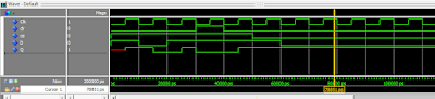
Simulation Waveform from Modelsim:
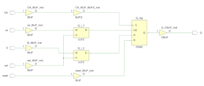
Schematic from Xilinx Vivado after Synthesis:

Note :- This flipflop entity is named with a "1" at the end because the name "FDCE" stands for a primitive component in Xilinx FPGAs which creates a synthesis error. You can see from the schematic that apart from few input and output buffers, the only flipflop used is called FDCE.