THIS ARTICLE IS APPLICABLE ONLY FOR XILINX ISE TOOL
This tutorial introduces some cool features of Xilinx ISE synthesis tool. I assume you're familiar with starting a project in Xilinx ISE and running simulations. If not, watch How to compile and simulate a VHDL code using Xilinx ISE first before continuing with this article.
Once you've successfully done functional simulation on your design, the next step would be to test it on a real fpga. The compiled VHDL code need to be translated or mapped into the resources available in the fpga. This is known as synthesis and can be done using Xilinx Synthesis Technology (XST), included in the Xilinx ISE software. XST generates Xilinx-specific net-list files known as NGC files. It's important to note that NGC files may vary even for the same VHDL code, depending on the chosen family and device. Each NGC file consists of two parts: logical design data and constraints.
Let's see how we can synthesis our design. Copy the VHDL code for a 4-bit counter with a reset input from here. Add this code to your Xilinx ISE project and click on Synthesis-XST to start the synthesis process. Once the design is synthesised successfully without any errors, a report will be generated with the following information.
View Synthesis Report:
To obtain the overall synthesis report, click on View Synthesis Report. This opens a file in a new tab with the extension .syr. From this file, you can gather the following information:
- Synthesis Options Summary
- HDL Compilation
- Design Hierarchy Analysis
- HDL Analysis
- HDL Synthesis
- HDL Synthesis Report
- Advanced HDL Synthesis
- Advanced HDL Synthesis Report
- Low Level Synthesis
- Partition Report
- Final Report
- Device utilization summary
- Partition Resource Summary
- Timing Summary
Additionally, synthesis results can be visualized by viewing two types of schematics:
View RTL schematic:
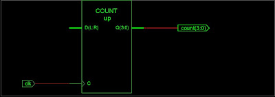
2) Click on View RTL schematic to see the RTL net-list generated by XST. The file opened will have the extension .ngr and is for viewing only. It provides a schematic representation of the pre-optimized design using generic symbols independent of the targeted Xilinx device, such as adders, multipliers, counters, AND gates, and OR gates, etc. In this case, the .ngr schematic will resemble this:
You'll notice that the schematic doesn't display any hardware elements. To identify the hardware elements used by tool for implementing this logic, you need to view the View Technology Schematic.
View Technology Schematic:
Refer to the figure below:
Looking at the diagram above, you can see that your design is implemented using one 4-input LUT (Lookup Table), one 3-input LUT, one 2-input LUT, and 4 FDCs (D flip-flops with asynchronous clear input). Additionally, other elements utilized include input buffers, output buffers, inverters, and so on.
Next, double-click on any of the LUTs (let's say LUT2). This opens a new window, displaying the following details:
- The schematic of the gate elements employed within that specific LUT.
- The Truth Table illustrating the function implemented by the LUT.
- The Karnaugh map corresponding to the truth table.


it helps me a lot...thank u.......
ReplyDelete